What Happened
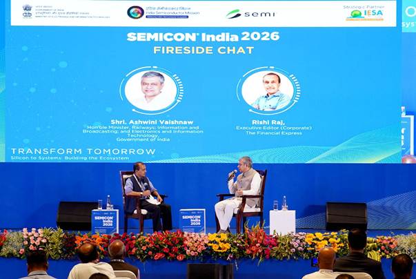
India has outlined the next phase of its semiconductor strategy under India Semiconductor Mission 2.0, with a stronger focus on building a complete domestic semiconductor ecosystem covering chip design, materials, manufacturing equipment, fabrication plants, assembly and packaging, research and development, and skilled human resources. The new direction was highlighted on 18 September 2026 during SEMICON India 2026.
Union Minister for Electronics and Information Technology Ashwini Vaishnaw said India's semiconductor programme has moved from establishing the basic foundation of the industry towards building the ecosystem at scale. According to the Ministry of Electronics and Information Technology, five semiconductor manufacturing plants in India have now commenced commercial production, marking an important transition from approved projects and construction activity towards actual production.
The government has divided the next phase of the semiconductor programme into six major pillars: Design; Materials and Machines; More Fabs; More ATMP units; Research and Development; and Talent. Together, these areas demonstrate that semiconductor self-reliance cannot be achieved simply by constructing fabrication plants. A semiconductor ecosystem requires design capabilities, specialised chemicals and materials, precision machinery, packaging and testing facilities, research institutions, trained engineers and technicians, reliable infrastructure and integration with global supply chains.
One of the most ambitious objectives announced under ISM 2.0 is the emergence of at least 200 chip-design companies. India already possesses a substantial semiconductor-design talent base because many global technology companies operate design and engineering centres in the country. The next challenge is to convert this human-resource advantage into greater creation of Indian semiconductor intellectual property and commercially successful chip products.
Electronic Design Automation tools are essential to modern chip design. EDA software allows engineers to design, simulate, verify and prepare integrated circuits for manufacturing. Such software is sophisticated and expensive, creating a significant entry barrier for start-ups and academic institutions. Under the first phase of the semiconductor mission, more than 105 chip-design start-ups received access to advanced industry-grade EDA tools. Twenty start-ups also received venture-capital funding support, according to the government.
The government now expects this design programme to expand further. The objective is not merely to increase the number of companies but to build domestic semiconductor intellectual property. Semiconductor IP can include specialised circuit designs, processor architectures, interfaces and other reusable design components that can be incorporated into electronic products. Ownership and development of such technology can increase the value captured domestically from the electronics industry.
Academic institutions are another important part of the strategy. Around 400 engineering colleges, including institutions located in smaller cities, have been provided access to industry-grade EDA tools. Students are receiving opportunities to develop designs and take some of them through the tape-out process. Tape-out is an important semiconductor term referring to the stage at which a completed chip design is prepared and sent for fabrication.
This approach is intended to reduce the traditional gap between classroom semiconductor education and actual industrial chip development. Students who work with professional design tools and understand the complete design-to-fabrication process can enter the semiconductor workforce with more practical experience.
India had initially established a target of training 85,000 semiconductor design engineers. According to the government, around 70,000 design engineers have already been trained within four years. Under ISM 2.0, the skill-development focus is expected to move beyond chip design towards system design and a wider range of semiconductor manufacturing skills.
The government has also identified increasing demand for cleanroom technicians and maintenance personnel. Semiconductor fabrication requires extremely controlled manufacturing environments because microscopic particles can damage semiconductor wafers and affect production yields. Cleanrooms therefore maintain carefully regulated levels of airborne particles, temperature, humidity and other environmental conditions.
The initial ISM 2.0 target of training one lakh technicians may have to be increased because of growing industry demand, according to the Minister. This illustrates an important feature of semiconductor industrialisation: the sector requires not only highly qualified chip designers but also technicians, equipment specialists, process engineers, maintenance professionals, material scientists and other skilled workers.
Precision manufacturing has consequently emerged as another important component of the semiconductor strategy. Semiconductor manufacturing equipment and supporting industrial systems require extremely high levels of accuracy. The electronics manufacturing ecosystem has already helped Indian MSMEs develop precision-manufacturing capabilities that can serve electronics, mobile manufacturing, aerospace, aviation, defence and semiconductor industries.
The government wants this capability to expand further under ISM 2.0. A multi-level training model is being developed for precision manufacturing, while greater emphasis is also being placed on applied research and development inside manufacturing plants. Applied R&D can help factories improve production processes, product quality, equipment performance and manufacturing efficiency.
Another important development is the beginning of commercial production at five semiconductor manufacturing plants. The government views this as evidence that the programme is moving beyond policy announcements and infrastructure construction into actual manufacturing. Semiconductor production must ultimately demonstrate competitiveness in both cost and quality because the industry operates through highly integrated international supply chains.
The semiconductor industry is one of the most globalised manufacturing systems in the world. A single chip may be designed in one country, use intellectual property developed in several others, depend on specialised chemicals and equipment from different economies, be fabricated elsewhere, packaged and tested in another location, and finally be incorporated into an electronic product manufactured somewhere else. Consequently, India's semiconductor strategy combines domestic capability-building with participation in global supply chains.
ATMP facilities form an important part of this ecosystem. ATMP stands for Assembly, Testing, Marking and Packaging. After semiconductor wafers are fabricated, individual chips need to be separated, packaged and tested before they can be incorporated into electronic systems. Building ATMP capability therefore adds another stage of semiconductor manufacturing within India.
According to the Ministry, Indian ATMP units are already exporting to Japan. Chips are also being incorporated into products exported to countries including Switzerland and Germany. These developments indicate that India's semiconductor programme is increasingly connected with international electronics supply chains.
The government has also highlighted the close relationship among semiconductors, electronics manufacturing and Artificial Intelligence. AI applications require substantial computing capacity, and specialised processors are central to AI servers and data-centre infrastructure. India is simultaneously seeking to expand electronics manufacturing and develop an ecosystem for AI servers, with major server manufacturers showing interest in manufacturing activities in the country.
This creates an interconnected industrial strategy. Domestic semiconductor capabilities can support electronics manufacturing; a larger electronics industry can create demand for chips; and growth in AI infrastructure can generate demand for servers, processors, memory, networking equipment and other electronic components.
Intellectual-property protection and trust are also important to the semiconductor sector. Chip designs and semiconductor manufacturing processes involve highly valuable proprietary technology. Companies therefore consider the security of intellectual property, supply-chain reliability, policy stability and trusted business relationships when deciding where to establish semiconductor operations.
For competitive-examination students, ISM 2.0 is important because it demonstrates the difference between semiconductor fabrication and a complete semiconductor ecosystem. A Fab manufactures semiconductor wafers, while ATMP facilities handle assembly, testing, marking and packaging. EDA tools are used for electronic chip design, and tape-out represents the transition of a completed design towards fabrication.
The latest developments also provide several direct current-affairs facts. Five semiconductor manufacturing plants have commenced commercial production. India is targeting at least 200 chip-design companies under ISM 2.0. More than 105 chip-design start-ups have received access to advanced EDA tools, while 20 start-ups have received venture-capital funding. Around 400 engineering colleges have access to industry-grade EDA tools, and approximately 70,000 semiconductor design engineers have been trained in four years.
The wider significance of ISM 2.0 lies in India's attempt to move higher in the global electronics value chain. Manufacturing finished electronic products is economically important, but greater value can potentially be generated by developing domestic capabilities in semiconductor design, intellectual property, fabrication, packaging, precision equipment, materials and advanced research. The next phase of the mission therefore seeks to create an interconnected semiconductor ecosystem rather than focusing on a single stage of chip production.
क्या हुआ?
भारत ने India Semiconductor Mission 2.0 के अंतर्गत अपनी सेमीकंडक्टर रणनीति के अगले चरण की रूपरेखा प्रस्तुत की है। इस चरण में Chip Design, Materials, Manufacturing Machines, Fabrication Plants, Assembly and Packaging, Research and Development तथा कुशल मानव संसाधन को जोड़कर एक संपूर्ण घरेलू सेमीकंडक्टर पारिस्थितिकी तंत्र विकसित करने पर अधिक जोर दिया जाएगा। 18 सितंबर 2026 को SEMICON India 2026 के दौरान इस दिशा से संबंधित महत्वपूर्ण जानकारी प्रस्तुत की गई।
केंद्रीय इलेक्ट्रॉनिक्स एवं सूचना प्रौद्योगिकी मंत्री अश्विनी वैष्णव के अनुसार भारत का सेमीकंडक्टर कार्यक्रम अब उद्योग की बुनियादी नींव तैयार करने के चरण से आगे बढ़कर बड़े स्तर पर संपूर्ण पारिस्थितिकी तंत्र विकसित करने की दिशा में जा रहा है। इलेक्ट्रॉनिक्स एवं सूचना प्रौद्योगिकी मंत्रालय के अनुसार भारत में पाँच सेमीकंडक्टर विनिर्माण संयंत्रों ने व्यावसायिक उत्पादन शुरू कर दिया है। यह स्वीकृत परियोजनाओं और निर्माण गतिविधियों से वास्तविक उत्पादन की ओर महत्वपूर्ण परिवर्तन को दर्शाता है।
सरकार ने सेमीकंडक्टर कार्यक्रम के अगले चरण को छह प्रमुख स्तंभों में विभाजित किया है — Design; Materials and Machines; More Fabs; More ATMP Units; Research and Development; तथा Talent। ये सभी क्षेत्र यह स्पष्ट करते हैं कि केवल Semiconductor Fabrication Plants स्थापित कर देने से सेमीकंडक्टर आत्मनिर्भरता प्राप्त नहीं की जा सकती। एक पूर्ण सेमीकंडक्टर व्यवस्था के लिए डिजाइन क्षमता, विशेष रसायन और सामग्री, अत्यंत सटीक मशीनें, Packaging और Testing Facilities, अनुसंधान संस्थान, प्रशिक्षित इंजीनियर और तकनीशियन तथा वैश्विक आपूर्ति शृंखला से जुड़ाव आवश्यक है।
ISM 2.0 के अंतर्गत घोषित सबसे महत्वपूर्ण लक्ष्यों में कम से कम 200 Chip Design Companies विकसित करने का लक्ष्य शामिल है। भारत के पास पहले से बड़ा Semiconductor Design Talent Base है क्योंकि अनेक वैश्विक तकनीकी कंपनियों के Design और Engineering Centres भारत में स्थित हैं। अब प्रमुख चुनौती इस मानव संसाधन क्षमता को भारतीय Semiconductor Intellectual Property और व्यावसायिक रूप से सफल Chip Products के निर्माण में बदलने की है।
Electronic Design Automation अर्थात EDA Tools आधुनिक Chip Design के लिए अत्यंत आवश्यक होते हैं। इन Software Tools के माध्यम से इंजीनियर Integrated Circuits का Design, Simulation और Verification कर सकते हैं तथा उन्हें Manufacturing के लिए तैयार कर सकते हैं। ऐसे Software अत्यधिक उन्नत और महंगे होते हैं, जिसके कारण Start-ups और शैक्षणिक संस्थानों के लिए इन तक पहुँच एक बड़ी चुनौती हो सकती है। Semiconductor Mission के पहले चरण में 105 से अधिक Chip Design Start-ups को उन्नत Industry-Grade EDA Tools तक पहुँच उपलब्ध कराई गई। सरकारी जानकारी के अनुसार 20 Start-ups को Venture Capital Funding भी प्राप्त हुई।
अब सरकार इस Design Programme को और विस्तारित करना चाहती है। उद्देश्य केवल कंपनियों की संख्या बढ़ाना नहीं बल्कि घरेलू Semiconductor Intellectual Property विकसित करना है। Semiconductor IP में विशेष Circuit Designs, Processor Architecture, Interfaces और अन्य पुनः उपयोग किए जा सकने वाले Design Components शामिल हो सकते हैं। ऐसी तकनीक का घरेलू विकास Electronics Industry से देश में उत्पन्न होने वाले आर्थिक मूल्य को बढ़ा सकता है।
शैक्षणिक संस्थान भी इस रणनीति का महत्वपूर्ण हिस्सा हैं। छोटे शहरों के संस्थानों सहित लगभग 400 Engineering Colleges को Industry-Grade EDA Tools तक पहुँच उपलब्ध कराई गई है। विद्यार्थियों को अपने Designs विकसित करने और उनमें से कुछ को Tape-Out प्रक्रिया तक ले जाने का अवसर भी दिया जा रहा है।
Tape-Out सेमीकंडक्टर क्षेत्र का महत्वपूर्ण तकनीकी शब्द है। इसका अर्थ उस चरण से है जब किसी Chip का Design पूरा हो जाता है और उसे Fabrication के लिए भेजने की तैयारी की जाती है। विद्यार्थियों को इस प्रक्रिया का अनुभव मिलने से पारंपरिक कक्षा शिक्षा और वास्तविक Semiconductor Industry के बीच अंतर कम किया जा सकता है।
भारत ने प्रारंभ में 85,000 Semiconductor Design Engineers को प्रशिक्षित करने का लक्ष्य रखा था। सरकार के अनुसार चार वर्षों में लगभग 70,000 Design Engineers को प्रशिक्षित किया जा चुका है। ISM 2.0 में कौशल विकास का दायरा केवल Chip Design तक सीमित नहीं रहेगा बल्कि System Design और Semiconductor Manufacturing से जुड़े अन्य कौशलों तक विस्तारित किया जाएगा।
सरकार ने Cleanroom Technicians और Maintenance Personnel की बढ़ती मांग को भी रेखांकित किया है। Semiconductor Fabrication के लिए अत्यंत नियंत्रित Manufacturing Environment आवश्यक होता है क्योंकि बहुत छोटे धूल कण भी Semiconductor Wafer को प्रभावित कर सकते हैं और उत्पादन की गुणवत्ता कम कर सकते हैं। इसलिए Cleanrooms में वायु में मौजूद कणों, तापमान, आर्द्रता और अन्य पर्यावरणीय स्थितियों को अत्यंत नियंत्रित रखा जाता है।
ISM 2.0 के अंतर्गत एक लाख Technicians को प्रशिक्षित करने का प्रारंभिक लक्ष्य उद्योग की बढ़ती मांग के कारण आगे बढ़ाना पड़ सकता है। इससे यह समझना महत्वपूर्ण है कि Semiconductor Industry को केवल उच्च शिक्षित Chip Designers की आवश्यकता नहीं होती। इसमें Technicians, Equipment Specialists, Process Engineers, Maintenance Professionals, Material Scientists और अन्य कुशल कर्मचारियों की भी बड़ी भूमिका होती है।
Precision Manufacturing इसी कारण भारत की Semiconductor Strategy का महत्वपूर्ण हिस्सा बनकर उभरा है। Semiconductor Manufacturing Equipment और उससे जुड़ी औद्योगिक प्रणालियों में अत्यंत उच्च स्तर की सटीकता की आवश्यकता होती है। भारत में Electronics Manufacturing Ecosystem ने विशेष रूप से MSMEs के बीच Precision Manufacturing क्षमता विकसित करने में सहायता की है। ये क्षमताएँ Electronics, Mobile Manufacturing, Aerospace, Aviation, Defence और Semiconductor जैसे अनेक क्षेत्रों में उपयोगी हो सकती हैं।
ISM 2.0 के अंतर्गत सरकार इस क्षमता को और विकसित करना चाहती है। Precision Manufacturing के लिए Multi-Level Training Model विकसित किया जा रहा है। इसके साथ Manufacturing Plants के अंदर Applied Research and Development पर भी अधिक जोर देने की बात कही गई है। Applied R&D के माध्यम से उत्पादन प्रक्रिया, उत्पाद गुणवत्ता, उपकरणों के प्रदर्शन और Manufacturing Efficiency में सुधार किया जा सकता है।
पाँच Semiconductor Manufacturing Plants में Commercial Production शुरू होना भी एक महत्वपूर्ण विकास है। सरकार इसे इस बात के संकेत के रूप में देखती है कि Semiconductor Programme अब केवल नीति घोषणाओं और Infrastructure Construction तक सीमित नहीं है बल्कि वास्तविक Manufacturing की दिशा में आगे बढ़ रहा है। वैश्विक बाजार में प्रतिस्पर्धा के लिए Semiconductor Production को Cost और Quality दोनों के स्तर पर सक्षम होना आवश्यक है।
Semiconductor Industry दुनिया की सबसे अधिक वैश्वीकृत Manufacturing Systems में से एक है। किसी Chip का Design एक देश में हो सकता है, उसमें कई देशों में विकसित Intellectual Property का उपयोग हो सकता है, उसके लिए विशेष Chemicals और Equipment अन्य देशों से आ सकते हैं, Fabrication किसी अन्य देश में हो सकती है और Packaging तथा Testing किसी अन्य स्थान पर की जा सकती है। अंततः वही Chip किसी दूसरे देश में तैयार Electronic Product में लग सकती है। इसलिए भारत की Semiconductor Strategy घरेलू क्षमता निर्माण के साथ Global Supply Chains में भागीदारी को भी जोड़ती है।
ATMP इस पारिस्थितिकी तंत्र का महत्वपूर्ण हिस्सा है। ATMP का पूरा रूप Assembly, Testing, Marking and Packaging है। Semiconductor Wafers के Fabrication के बाद अलग-अलग Chips को अलग करना, Package करना और उनकी Testing करना आवश्यक होता है। इसके बाद ही उन्हें Electronic Systems में उपयोग किया जा सकता है। भारत में ATMP क्षमता विकसित होने से Semiconductor Manufacturing Value Chain का एक और महत्वपूर्ण चरण देश में स्थापित होता है।
मंत्रालय के अनुसार भारत की ATMP Units जापान को निर्यात कर रही हैं। भारत में बने Chips को ऐसे Products में भी शामिल किया जा रहा है जिनका निर्यात Switzerland और Germany जैसे देशों में किया जाता है। यह भारत की Semiconductor Manufacturing को अंतरराष्ट्रीय Electronics Supply Chains से जोड़ने का संकेत देता है।
सरकार ने Semiconductors, Electronics Manufacturing और Artificial Intelligence के बीच निकट संबंध पर भी जोर दिया है। AI Applications के लिए बड़े पैमाने पर Computing Capacity आवश्यक होती है और AI Servers तथा Data Centres के लिए विशेष Processors महत्वपूर्ण होते हैं। भारत Electronics Manufacturing के साथ AI Server Manufacturing Ecosystem का भी विस्तार करना चाहता है।
इससे एक परस्पर जुड़ी औद्योगिक रणनीति बनती है। घरेलू Semiconductor Capability Electronics Manufacturing को समर्थन दे सकती है; बड़ी Electronics Industry Chips की घरेलू मांग उत्पन्न कर सकती है; और AI Infrastructure का विस्तार Servers, Processors, Memory, Networking Equipment तथा अन्य Electronic Components की मांग बढ़ा सकता है।
Intellectual Property Protection और Trust भी Semiconductor Industry के महत्वपूर्ण तत्व हैं। Chip Designs और Semiconductor Manufacturing Processes में अत्यधिक मूल्यवान स्वामित्व तकनीक शामिल होती है। इसलिए कंपनियाँ किसी देश में निवेश का निर्णय लेते समय Intellectual Property की सुरक्षा, Supply Chain Reliability और नीतिगत स्थिरता जैसे कारकों पर विचार करती हैं।
प्रतियोगी परीक्षाओं के विद्यार्थियों के लिए ISM 2.0 इसलिए महत्वपूर्ण है क्योंकि यह Semiconductor Fabrication और संपूर्ण Semiconductor Ecosystem के बीच अंतर समझने में सहायता करता है। Fab Semiconductor Wafers का निर्माण करता है, जबकि ATMP Facilities Assembly, Testing, Marking और Packaging का कार्य करती हैं। EDA Tools Electronic Chip Design के लिए उपयोग किए जाते हैं और Tape-Out पूर्ण Chip Design को Fabrication की ओर ले जाने वाला महत्वपूर्ण चरण है।
नवीनतम घटनाक्रम से कई प्रत्यक्ष समसामयिक तथ्य भी प्राप्त होते हैं। पाँच Semiconductor Manufacturing Plants ने Commercial Production शुरू कर दिया है। ISM 2.0 के अंतर्गत भारत कम से कम 200 Chip Design Companies विकसित करने का लक्ष्य रख रहा है। 105 से अधिक Chip Design Start-ups को Advanced EDA Tools तक पहुँच मिली है और 20 Start-ups को Venture Capital Funding प्राप्त हुई है। लगभग 400 Engineering Colleges को Industry-Grade EDA Tools उपलब्ध कराए गए हैं तथा चार वर्षों में लगभग 70,000 Semiconductor Design Engineers को प्रशिक्षित किया गया है।
ISM 2.0 का व्यापक महत्व भारत को Global Electronics Value Chain में उच्च स्तर पर पहुँचाने के प्रयास में है। Finished Electronic Products का निर्माण महत्वपूर्ण है, लेकिन Semiconductor Design, Intellectual Property, Fabrication, Packaging, Precision Equipment, Materials और Advanced Research जैसी क्षमताओं के विकास से अधिक आर्थिक मूल्य देश के भीतर उत्पन्न किया जा सकता है। इसलिए मिशन का अगला चरण केवल Chip Production के किसी एक हिस्से पर ध्यान देने के बजाय परस्पर जुड़े पूर्ण Semiconductor Ecosystem के निर्माण पर केंद्रित है।
Key Facts
• India Semiconductor Mission 2.0 will focus on developing a complete semiconductor ecosystem.
• The six pillars of ISM 2.0 are Design, Materials and Machines, More Fabs, More ATMP units, R&D and Talent.
• Five semiconductor manufacturing plants in India have commenced commercial production.
• India is targeting the emergence of at least 200 chip-design companies under ISM 2.0.
• More than 105 chip-design start-ups have received access to industry-grade EDA tools.
• Twenty semiconductor-design start-ups have received venture-capital funding.
• Around 400 engineering colleges have received access to industry-grade EDA tools.
• India originally targeted training 85,000 semiconductor design engineers.
• Around 70,000 design engineers have already been trained within four years.
• ISM 2.0 will expand skilling from chip design towards system design.
• The government has an initial target of training one lakh technicians under ISM 2.0.
• Demand for cleanroom technicians and semiconductor maintenance personnel is increasing.
• Precision manufacturing is being developed as an important supporting capability for semiconductor manufacturing.
• Indian ATMP units are already exporting to Japan.
• Chips are also being incorporated into products exported to Switzerland and Germany.
मुख्य तथ्य
• India Semiconductor Mission 2.0 का उद्देश्य संपूर्ण Semiconductor Ecosystem विकसित करना है।
• ISM 2.0 के छह प्रमुख स्तंभ Design, Materials and Machines, More Fabs, More ATMP Units, R&D और Talent हैं।
• भारत में पाँच Semiconductor Manufacturing Plants ने Commercial Production शुरू कर दिया है।
• ISM 2.0 के अंतर्गत कम से कम 200 Chip Design Companies विकसित करने का लक्ष्य है।
• 105 से अधिक Chip Design Start-ups को Industry-Grade EDA Tools तक पहुँच मिली है।
• 20 Semiconductor Design Start-ups को Venture Capital Funding मिली है।
• लगभग 400 Engineering Colleges को Industry-Grade EDA Tools तक पहुँच प्रदान की गई है।
• भारत ने प्रारंभ में 85,000 Semiconductor Design Engineers को प्रशिक्षित करने का लक्ष्य रखा था।
• चार वर्षों में लगभग 70,000 Design Engineers को प्रशिक्षित किया जा चुका है।
• ISM 2.0 में Skill Development को Chip Design से System Design तक विस्तारित किया जाएगा।
• ISM 2.0 में प्रारंभिक रूप से एक लाख Technicians को प्रशिक्षित करने का लक्ष्य रखा गया है।
• Cleanroom Technicians और Semiconductor Maintenance Personnel की मांग बढ़ रही है।
• Precision Manufacturing को Semiconductor Manufacturing की महत्वपूर्ण सहायक क्षमता के रूप में विकसित किया जा रहा है।
• भारतीय ATMP Units जापान को निर्यात कर रही हैं।
• भारत में निर्मित Chips को Switzerland और Germany को निर्यात होने वाले Products में भी शामिल किया जा रहा है।
Background
India Semiconductor Mission was created to develop domestic semiconductor and display manufacturing capabilities and strengthen India's position in the global electronics value chain. Semiconductor production requires much more than fabrication plants: design software, intellectual property, specialised materials, precision machinery, fabrication, assembly and testing, research capabilities and a skilled workforce are all required. ISM 2.0 therefore broadens the approach from establishing individual projects towards building an interconnected semiconductor ecosystem.
पृष्ठभूमि
India Semiconductor Mission का उद्देश्य घरेलू Semiconductor और Display Manufacturing क्षमताओं का विकास करना तथा Global Electronics Value Chain में भारत की स्थिति मजबूत करना है। Semiconductor Production के लिए केवल Fabrication Plants पर्याप्त नहीं होते। Design Software, Intellectual Property, विशेष Materials, Precision Machinery, Fabrication, Assembly and Testing, Research Capability और कुशल Workforce सभी आवश्यक होते हैं। इसलिए ISM 2.0 अलग-अलग परियोजनाओं की स्थापना से आगे बढ़कर परस्पर जुड़े संपूर्ण Semiconductor Ecosystem के निर्माण पर जोर देता है।
Why It Matters
Semiconductors are foundational components of smartphones, computers, vehicles, telecommunications equipment, defence systems, industrial machines, medical devices, data centres and artificial-intelligence infrastructure. Developing capabilities across semiconductor design, manufacturing, packaging, materials and equipment can reduce strategic vulnerabilities while creating high-skill employment and opportunities for Indian companies. The emphasis on 200 design companies, precision manufacturing and industry-grade training also indicates an attempt to move India from electronics assembly towards higher-value technology and intellectual-property creation.
यह क्यों महत्वपूर्ण है?
Semiconductors Smartphones, Computers, Vehicles, Telecommunication Equipment, Defence Systems, Industrial Machines, Medical Devices, Data Centres और Artificial Intelligence Infrastructure के मूलभूत घटक हैं। Semiconductor Design, Manufacturing, Packaging, Materials और Equipment में क्षमता विकसित करने से सामरिक निर्भरता कम करने के साथ उच्च कौशल वाले रोजगार और भारतीय कंपनियों के लिए नए अवसर उत्पन्न हो सकते हैं। 200 Design Companies, Precision Manufacturing और Industry-Grade Training पर जोर भारत को केवल Electronics Assembly से आगे बढ़ाकर उच्च मूल्य वाली Technology और Intellectual Property Creation की दिशा में ले जाने के प्रयास को दर्शाता है।
Exam Connection
Important for UPSC Prelims, GS-III Science & Technology and Economy, SSC, Railway, Banking and State PCS. Remember: ISM 2.0 has six pillars — Design, Materials and Machines, More Fabs, More ATMP units, R&D and Talent. Five semiconductor manufacturing plants have begun commercial production. India is targeting at least 200 chip-design companies. More than 105 start-ups and around 400 engineering colleges have received access to industry-grade EDA tools, while around 70,000 design engineers have been trained. Also remember: EDA means Electronic Design Automation; ATMP means Assembly, Testing, Marking and Packaging; and tape-out is an important stage between completed chip design and fabrication.
परीक्षा से संबंध
UPSC प्रारंभिक परीक्षा, GS-III विज्ञान एवं प्रौद्योगिकी तथा अर्थव्यवस्था, SSC, Railway, Banking और State PCS के लिए महत्वपूर्ण। याद रखें: ISM 2.0 के छह स्तंभ हैं — Design, Materials and Machines, More Fabs, More ATMP Units, R&D और Talent। पाँच Semiconductor Manufacturing Plants ने Commercial Production शुरू किया है। भारत कम से कम 200 Chip Design Companies विकसित करने का लक्ष्य रख रहा है। 105 से अधिक Start-ups और लगभग 400 Engineering Colleges को Industry-Grade EDA Tools तक पहुँच मिली है तथा लगभग 70,000 Design Engineers को प्रशिक्षित किया गया है। EDA का अर्थ Electronic Design Automation, ATMP का अर्थ Assembly, Testing, Marking and Packaging है तथा Tape-Out पूर्ण Chip Design और Fabrication के बीच महत्वपूर्ण चरण है।