What Happened
1. Why in News?
On 5 October 2026, the Technology Development Board under the Department of Science and Technology announced an agreement with BigEndian Semiconductors, a Bengaluru-based company, to provide ₹130 crore in financial support for Project VeerAI. The project aims to develop an indigenous AI Vision System-on-Chip for secure and intelligent camera applications. The announcement is important because it connects India's semiconductor ambitions with artificial intelligence, surveillance technology and technological self-reliance.
2. Official Announcement
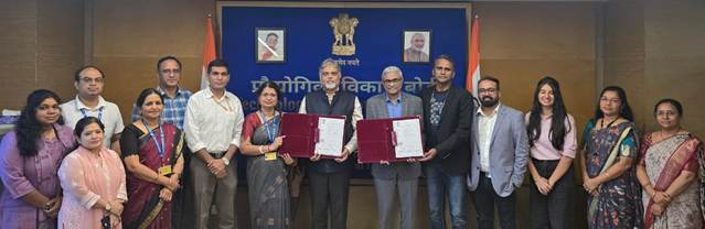
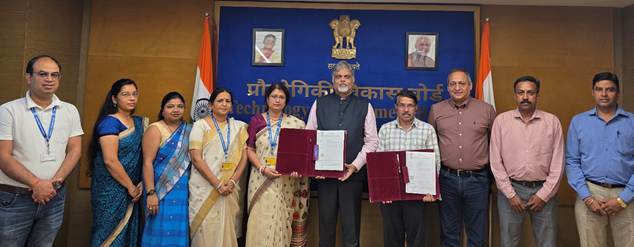
The Ministry of Science and Technology published the announcement through the Press Information Bureau on 5 October 2026. The agreement was signed by the Technology Development Board and BigEndian Semiconductors under the Research Development and Innovation Fund. The official release described the financial structure, technological objectives, potential applications and commercialisation roadmap.
3. What Is Project VeerAI?
Project VeerAI is an Indian semiconductor development initiative focused on creating a camera-oriented AI Vision System-on-Chip. Its purpose is to integrate intelligent image processing, connectivity and security capabilities into an application-specific semiconductor platform. The project is initially directed towards CCTV and surveillance applications.
4. Implementing Company
BigEndian Semiconductors, based in Bengaluru, Karnataka, is the company undertaking the project. It is responsible for progressing the technology through further development, validation, integration, testing and scale-up activities. The announcement does not establish that the final commercial product has already been launched.
5. Government Institution Involved
The Technology Development Board, abbreviated TDB, signed the agreement. TDB operates under the Department of Science and Technology, Government of India. Its role in this initiative is to provide financial support for technology development and movement towards commercial readiness.
6. Financial Support
The announced financial support is ₹130 crore. This amount is being provided under the Research Development and Innovation Fund. It represents support for the project rather than a statement that the complete semiconductor development programme has already been finished.
7. Total Project Cost
The total cost of Project VeerAI is ₹260 crore. The announced TDB support of ₹130 crore equals 50% of this project cost. The official release does not provide a complete itemised breakdown of every other funding contribution.
8. Funding Mechanism
The support will be provided through Optional Convertible Debt, abbreviated OCD. This is a financing structure under which debt may be convertible according to applicable contractual conditions. It should not be confused with a conventional unconditional grant.
9. Research Development and Innovation Fund
The RDI Fund supports technology development and innovation. In Project VeerAI, it is being used to assist the progression of a semiconductor technology towards commercial deployment. This illustrates the importance of financing during the period between research development and market introduction.
10. What Is a Semiconductor?
A semiconductor is a material whose electrical conductivity can be controlled through material properties and engineering techniques. Silicon is widely used in semiconductor manufacturing. Semiconductor devices form the basis of modern computing, communication, sensors and electronic control systems.
11. What Is a Semiconductor Chip?
A semiconductor chip is an electronic component containing integrated circuits that perform particular functions. Depending on design, chips may process data, store information, manage power or support communications. Modern devices often contain multiple specialised chips.
12. What Is a System-on-Chip?
A System-on-Chip, or SoC, integrates several electronic functions into a single chip. These may include processors, memory interfaces, input-output systems and specialised accelerators. The precise components depend on the product's intended application.
13. What Is an AI Vision SoC?
An AI Vision SoC is designed to support visual-data processing and artificial intelligence tasks. It may perform functions such as image processing and AI-based analysis closer to the camera or device. Project VeerAI aims to develop this type of specialised semiconductor platform.
14. Meaning of Application-Specific Technology
Application-specific technology is designed around the requirements of particular tasks rather than trying to serve every possible computing purpose. Project VeerAI focuses initially on intelligent camera and surveillance requirements. Such specialisation can help align chip architecture with practical product needs.
15. Initial Focus on CCTV
The first major application identified in the announcement is CCTV surveillance. CCTV stands for Closed-Circuit Television. Modern CCTV systems may combine cameras, storage, communication networks and software to support monitoring and security functions.
16. Artificial Intelligence in Cameras
AI-enabled cameras can potentially analyse visual information using computational models. Depending on the implemented features, they may support automated detection or other intelligent functions. The official release did not disclose a complete final list of algorithms or guarantee specific accuracy levels for Project VeerAI.
17. Security and Privacy
The proposed platform is designed to combine AI processing with security, privacy and connectivity capabilities. These features are relevant because camera systems may process sensitive visual information. Actual privacy protection depends on the final architecture, software, configuration and operational practices.
18. Indigenous Technology Platform
The project seeks to establish an Indian technology platform for application-specific AI chips. Indigenous development can strengthen domestic design expertise and reduce dependence on selected external technology suppliers. The announcement does not claim that every component or manufacturing step is already entirely domestic.
19. Technology Readiness Level
Technology Readiness Level, abbreviated TRL, is a framework used to describe the maturity of a technology. It helps distinguish early concepts and prototypes from systems that have been tested and demonstrated in realistic operating conditions.
20. Starting Readiness Level
The official announcement identifies TRL-5 as the project's starting point for the planned advancement. TRL-5 generally indicates that relevant technology components have been validated in a relevant environment. It does not imply that the final product has completed commercial deployment.
21. Target Readiness Level
The project aims to reach TRL-9. This level generally corresponds to an actual system proven through successful operational use. Reaching TRL-9 is a project objective, not an achievement already confirmed by the October 2026 announcement.
22. Development Activities
BigEndian Semiconductors is expected to undertake further technology development, validation, integration, testing and scale-up. These stages are important because a promising semiconductor design must be transformed into a reliable and deployable product.
23. Commercialisation
Commercialisation refers to bringing a technology into practical market use. The project aims to progress from advanced development towards commercial readiness. Successful commercialisation would require technical validation, product development and suitable market conditions.
24. VLSI Design
VLSI stands for Very Large Scale Integration. It refers to the integration of very large numbers of electronic components, particularly transistors, into integrated circuits. VLSI design is a foundational field in semiconductor engineering.
25. India's Semiconductor Talent
The official announcement highlighted India's growing VLSI design and semiconductor talent. Project VeerAI seeks to convert domestic design expertise into a scalable product platform. This connection between skilled engineers and commercial products is central to building a sustainable semiconductor industry.
26. Potential Defence Applications
The project roadmap identifies defence as a potential future application area. Intelligent visual processing and secure electronics can be relevant to various defence systems. However, the October announcement did not establish that the chip has already been inducted into a military platform.
27. Potential Automotive Applications
The roadmap also includes automotive applications. Modern vehicles increasingly use electronic systems and sensors. Vision-processing chips may support certain vehicle-related functions, although the exact applications and performance specifications of the future VeerAI product have not been disclosed.
28. Potential Industrial Applications
Industrial systems use sensors, automation and computing to monitor processes and equipment. Application-specific AI vision technology may eventually be adapted to selected industrial tasks. The project's initial announced emphasis remains CCTV and surveillance.
29. Potential Medical Applications
Medical technology is another sector identified in the roadmap. Image processing and specialised electronics can be relevant to medical devices, but clinical suitability would require application-specific development, validation and applicable regulatory approvals.
30. India and the Global South
The project is initially intended for CCTV and surveillance applications in India and the Global South. The expression Global South generally refers to developing and emerging economies, although it is not a rigid geographical classification. The project therefore has potential relevance beyond the domestic market.
31. Supply-Chain Dependence
Semiconductor supply chains involve design tools, intellectual property, materials, manufacturing equipment, fabrication, packaging and testing. Dependence on external suppliers can create vulnerabilities. Developing domestic expertise in selected parts of this chain can strengthen resilience.
32. Technological Sovereignty
Technological sovereignty refers to a country's capacity to develop, control and maintain important technological capabilities. The VeerAI initiative is relevant because secure application-specific chips can support greater domestic expertise in critical electronic systems.
33. Edge AI
Edge AI refers to running artificial intelligence computations on or near the device where data is generated rather than relying entirely on remote cloud servers. Camera-focused AI chips can be relevant to this approach. The official announcement described onboard AI processing capabilities but did not provide detailed benchmarks.
34. Why Specialised Chips Matter
Specialised chips are designed to perform selected tasks efficiently. They may offer advantages in power use, processing speed or system integration when compared with less specialised approaches, depending on design. Project VeerAI aims to address specific camera and surveillance requirements rather than every computing application.
35. Importance for Research and Industry
The project links public financial support with private-sector technology development. Such arrangements can help companies undertake expensive engineering and validation activities. Their ultimate success depends on technical execution and commercial outcomes.
36. Importance for Students
The announcement is relevant to students studying computer science, electronics, electrical engineering, artificial intelligence and cybersecurity. Important learning areas include semiconductor fundamentals, SoC architecture, VLSI, embedded systems, AI vision, technology readiness levels and research commercialisation.
37. Importance for Competitive Examinations
UPSC, SSC, Railway and State PCS examinations may ask about the responsible ministry, implementing organisation, project name, financial support, total cost, TRL targets and semiconductor terminology. Candidates should distinguish between a project announcement and a completed commercial product.
38. Important Numerical Facts
Government support: ₹130 crore. Total project cost: ₹260 crore. Planned technology advancement: TRL-5 to TRL-9. Announcement date: 5 October 2026. Implementing company: BigEndian Semiconductors, Bengaluru.
39. What Has Been Confirmed?
The official announcement confirms an agreement for financial support, the project's intended AI Vision SoC technology, the funding mechanism and the planned development path. It does not confirm that a finished chip has entered mass production or that the proposed future sectoral applications have already been commercially deployed.
40. Overall Significance
Project VeerAI is an important Indian initiative at the intersection of artificial intelligence, semiconductor design and secure electronics. The ₹130 crore RDI support is intended to help transform a camera-focused AI chip technology into a commercially deployable platform. Its success could strengthen domestic semiconductor design capabilities and support India's broader technological self-reliance objectives.
क्या हुआ?
1. चर्चा में क्यों?
5 अक्टूबर 2026 को विज्ञान एवं प्रौद्योगिकी विभाग के अंतर्गत प्रौद्योगिकी विकास बोर्ड ने बेंगलुरु स्थित बिगएंडियन सेमीकंडक्टर्स के साथ परियोजना वीरएआई के लिए ₹130 करोड़ की वित्तीय सहायता का समझौता करने की घोषणा की। परियोजना का उद्देश्य सुरक्षित और बुद्धिमान कैमरा अनुप्रयोगों के लिए स्वदेशी कृत्रिम बुद्धिमत्ता आधारित विजन सिस्टम-ऑन-चिप विकसित करना है। यह घोषणा महत्वपूर्ण है क्योंकि यह भारत की सेमीकंडक्टर महत्वाकांक्षाओं को कृत्रिम बुद्धिमत्ता, निगरानी तकनीक और तकनीकी आत्मनिर्भरता से जोड़ती है।
2. आधिकारिक घोषणा
विज्ञान एवं प्रौद्योगिकी मंत्रालय ने 5 अक्टूबर 2026 को प्रेस सूचना ब्यूरो के माध्यम से यह घोषणा प्रकाशित की। समझौता प्रौद्योगिकी विकास बोर्ड और बिगएंडियन सेमीकंडक्टर्स के बीच अनुसंधान, विकास और नवाचार कोष के अंतर्गत किया गया। आधिकारिक विज्ञप्ति में वित्तीय व्यवस्था, तकनीकी उद्देश्य, संभावित उपयोग और व्यावसायीकरण की योजना बताई गई।
3. परियोजना वीरएआई क्या है?
परियोजना वीरएआई एक भारतीय सेमीकंडक्टर विकास पहल है, जिसका उद्देश्य कैमरा केंद्रित कृत्रिम बुद्धिमत्ता विजन सिस्टम-ऑन-चिप विकसित करना है। इसका लक्ष्य बुद्धिमान छवि प्रसंस्करण, संपर्क व्यवस्था और सुरक्षा क्षमताओं को विशेष अनुप्रयोगों के लिए विकसित एक चिप में एकीकृत करना है। परियोजना का प्रारंभिक ध्यान सीसीटीवी और निगरानी अनुप्रयोगों पर है।
4. कार्यान्वयन करने वाली कंपनी
कर्नाटक के बेंगलुरु में स्थित बिगएंडियन सेमीकंडक्टर्स परियोजना पर काम करने वाली कंपनी है। यह आगे के विकास, सत्यापन, एकीकरण, परीक्षण और बड़े स्तर पर उत्पादन की तैयारी से संबंधित गतिविधियां करेगी। घोषणा से यह स्थापित नहीं होता कि अंतिम व्यावसायिक उत्पाद पहले ही बाजार में उपलब्ध हो चुका है।
5. संबंधित सरकारी संस्था
प्रौद्योगिकी विकास बोर्ड अर्थात TDB ने समझौते पर हस्ताक्षर किए। यह भारत सरकार के विज्ञान एवं प्रौद्योगिकी विभाग के अंतर्गत कार्य करता है। इस पहल में इसकी भूमिका प्रौद्योगिकी विकास और व्यावसायिक तैयारी की दिशा में वित्तीय सहायता प्रदान करना है।
6. वित्तीय सहायता
घोषित वित्तीय सहायता ₹130 करोड़ है। यह राशि अनुसंधान, विकास और नवाचार कोष के अंतर्गत प्रदान की जाएगी। यह परियोजना के विकास के लिए सहायता है, न कि इस बात की पुष्टि कि पूरा सेमीकंडक्टर विकास कार्यक्रम पहले ही समाप्त हो चुका है।
7. परियोजना की कुल लागत
परियोजना वीरएआई की कुल लागत ₹260 करोड़ है। घोषित ₹130 करोड़ की सहायता कुल लागत के 50 प्रतिशत के बराबर है। आधिकारिक विज्ञप्ति में शेष सभी वित्तीय योगदानों का विस्तृत मदवार विवरण नहीं दिया गया।
8. वित्तपोषण की व्यवस्था
सहायता वैकल्पिक परिवर्तनीय ऋण अर्थात Optional Convertible Debt के माध्यम से दी जाएगी। यह ऐसी वित्तीय व्यवस्था है जिसमें लागू अनुबंधीय शर्तों के अनुसार ऋण का रूपांतरण संभव हो सकता है। इसे सामान्य बिना शर्त अनुदान के समान नहीं समझना चाहिए।
9. अनुसंधान, विकास और नवाचार कोष
RDI कोष प्रौद्योगिकी विकास और नवाचार का समर्थन करता है। परियोजना वीरएआई में इसका उपयोग सेमीकंडक्टर तकनीक को व्यावसायिक उपयोग के स्तर तक पहुंचाने में सहायता के लिए किया जा रहा है। यह अनुसंधान विकास और बाजार में उत्पाद लाने के बीच वित्तपोषण के महत्व को दर्शाता है।
10. सेमीकंडक्टर क्या है?
सेमीकंडक्टर ऐसी सामग्री है जिसकी विद्युत चालकता को उसके गुणों और अभियांत्रिक तकनीकों के माध्यम से नियंत्रित किया जा सकता है। सिलिकॉन सेमीकंडक्टर निर्माण में व्यापक रूप से उपयोग किया जाता है। सेमीकंडक्टर उपकरण आधुनिक कंप्यूटिंग, संचार, संवेदकों और इलेक्ट्रॉनिक नियंत्रण प्रणालियों का आधार हैं।
11. सेमीकंडक्टर चिप क्या है?
सेमीकंडक्टर चिप एक इलेक्ट्रॉनिक घटक है जिसमें विशेष कार्य करने वाले एकीकृत परिपथ होते हैं। डिजाइन के अनुसार चिप आंकड़ों का प्रसंस्करण, जानकारी का भंडारण, ऊर्जा प्रबंधन या संचार का कार्य कर सकती है। आधुनिक उपकरणों में अक्सर कई विशेष चिप लगी होती हैं।
12. सिस्टम-ऑन-चिप क्या है?
सिस्टम-ऑन-चिप अर्थात SoC कई इलेक्ट्रॉनिक कार्यों को एक ही चिप में एकीकृत करता है। इनमें प्रोसेसर, स्मृति से संबंधित इंटरफेस, इनपुट-आउटपुट प्रणालियां और विशेष गणना इकाइयां शामिल हो सकती हैं। वास्तविक घटक उत्पाद के निर्धारित उपयोग पर निर्भर करते हैं।
13. AI विजन SoC क्या है?
AI विजन SoC दृश्य आंकड़ों के प्रसंस्करण और कृत्रिम बुद्धिमत्ता से संबंधित कार्यों के लिए विकसित की जाती है। यह कैमरे या उपकरण के निकट छवि प्रसंस्करण और AI आधारित विश्लेषण कर सकती है। परियोजना वीरएआई का उद्देश्य इसी प्रकार की विशेष सेमीकंडक्टर प्रणाली विकसित करना है।
14. विशेष अनुप्रयोग वाली तकनीक का अर्थ
विशेष अनुप्रयोग वाली तकनीक हर प्रकार के कंप्यूटिंग कार्य के बजाय निर्धारित आवश्यकताओं को ध्यान में रखकर विकसित की जाती है। परियोजना वीरएआई का प्रारंभिक ध्यान बुद्धिमान कैमरा और निगरानी आवश्यकताओं पर है। ऐसी विशेषज्ञता चिप के डिजाइन को वास्तविक उत्पाद की जरूरतों के अनुरूप बनाने में सहायता कर सकती है।
15. सीसीटीवी पर प्रारंभिक ध्यान
घोषणा में बताया गया पहला प्रमुख उपयोग सीसीटीवी निगरानी है। CCTV का पूरा नाम Closed-Circuit Television है। आधुनिक सीसीटीवी प्रणालियां निगरानी और सुरक्षा के लिए कैमरे, भंडारण, संचार नेटवर्क और सॉफ्टवेयर का उपयोग कर सकती हैं।
16. कैमरों में कृत्रिम बुद्धिमत्ता
AI युक्त कैमरे गणनात्मक मॉडल का उपयोग करके दृश्य जानकारी का विश्लेषण कर सकते हैं। उपलब्ध सुविधाओं के अनुसार वे स्वचालित पहचान या अन्य बुद्धिमान कार्यों में सहायता कर सकते हैं। आधिकारिक विज्ञप्ति में वीरएआई के सभी अंतिम एल्गोरिदम या किसी निश्चित सटीकता स्तर की जानकारी नहीं दी गई।
17. सुरक्षा और गोपनीयता
प्रस्तावित प्लेटफॉर्म में AI प्रसंस्करण के साथ सुरक्षा, गोपनीयता और संपर्क क्षमताएं शामिल करने की योजना है। ये विशेषताएं महत्वपूर्ण हैं क्योंकि कैमरा प्रणालियां संवेदनशील दृश्य जानकारी का प्रसंस्करण कर सकती हैं। वास्तविक गोपनीयता सुरक्षा अंतिम डिजाइन, सॉफ्टवेयर, विन्यास और परिचालन प्रक्रियाओं पर निर्भर करेगी।
18. स्वदेशी प्रौद्योगिकी प्लेटफॉर्म
परियोजना का उद्देश्य विशेष AI चिप के लिए भारतीय प्रौद्योगिकी प्लेटफॉर्म स्थापित करना है। स्वदेशी विकास घरेलू डिजाइन विशेषज्ञता मजबूत कर सकता है और कुछ बाहरी तकनीकी आपूर्तिकर्ताओं पर निर्भरता कम कर सकता है। घोषणा में यह दावा नहीं किया गया कि प्रत्येक घटक या विनिर्माण चरण पहले ही पूरी तरह घरेलू हो चुका है।
19. प्रौद्योगिकी तत्परता स्तर
Technology Readiness Level अर्थात TRL एक ऐसी प्रणाली है जिसका उपयोग किसी प्रौद्योगिकी की परिपक्वता बताने के लिए किया जाता है। इससे शुरुआती अवधारणाओं और प्रोटोटाइप को वास्तविक परिस्थितियों में जांची गई प्रणालियों से अलग समझने में सहायता मिलती है।
20. प्रारंभिक तत्परता स्तर
आधिकारिक घोषणा में नियोजित प्रगति का शुरुआती स्तर TRL-5 बताया गया। सामान्यतः TRL-5 का अर्थ संबंधित वातावरण में तकनीकी घटकों का सत्यापन होना है। इसका अर्थ अंतिम उत्पाद का व्यावसायिक उपयोग पूरा होना नहीं है।
21. लक्षित तत्परता स्तर
परियोजना का लक्ष्य TRL-9 तक पहुंचना है। यह स्तर सामान्यतः वास्तविक परिचालन में सफलतापूर्वक सिद्ध प्रणाली से संबंधित होता है। TRL-9 तक पहुंचना परियोजना का उद्देश्य है, अक्टूबर 2026 की घोषणा में पहले से सिद्ध उपलब्धि नहीं।
22. विकास संबंधी गतिविधियां
बिगएंडियन सेमीकंडक्टर्स आगे प्रौद्योगिकी विकास, सत्यापन, एकीकरण, परीक्षण और बड़े स्तर पर उपयोग की तैयारी करेगी। ये चरण महत्वपूर्ण हैं क्योंकि आशाजनक सेमीकंडक्टर डिजाइन को विश्वसनीय और उपयोग योग्य उत्पाद में बदलना आवश्यक होता है।
23. व्यावसायीकरण
व्यावसायीकरण का अर्थ किसी प्रौद्योगिकी को वास्तविक बाजार उपयोग में लाना है। परियोजना का उद्देश्य उन्नत विकास की अवस्था से व्यावसायिक तैयारी की ओर बढ़ना है। सफल व्यावसायीकरण के लिए तकनीकी सत्यापन, उत्पाद विकास और उपयुक्त बाजार परिस्थितियां आवश्यक होंगी।
24. VLSI डिजाइन
VLSI का पूरा नाम Very Large Scale Integration है। इसका अर्थ बहुत बड़ी संख्या में इलेक्ट्रॉनिक घटकों, विशेषकर ट्रांजिस्टरों, को एकीकृत परिपथ में समाहित करना है। VLSI डिजाइन सेमीकंडक्टर अभियांत्रिकी का आधारभूत क्षेत्र है।
25. भारत की सेमीकंडक्टर प्रतिभा
आधिकारिक घोषणा में भारत की बढ़ती VLSI डिजाइन और सेमीकंडक्टर विशेषज्ञता का उल्लेख किया गया। परियोजना वीरएआई घरेलू डिजाइन क्षमताओं को बड़े स्तर पर उपयोग योग्य उत्पाद में बदलना चाहती है। कुशल अभियंताओं और व्यावसायिक उत्पादों के बीच यह संबंध स्थायी सेमीकंडक्टर उद्योग बनाने के लिए महत्वपूर्ण है।
26. रक्षा क्षेत्र में संभावित उपयोग
परियोजना की भविष्य की योजना में रक्षा क्षेत्र को संभावित उपयोग के रूप में शामिल किया गया है। बुद्धिमान दृश्य प्रसंस्करण और सुरक्षित इलेक्ट्रॉनिक्स विभिन्न रक्षा प्रणालियों में उपयोगी हो सकते हैं। हालांकि अक्टूबर की घोषणा में यह स्थापित नहीं हुआ कि चिप को पहले ही किसी सैन्य प्लेटफॉर्म में शामिल किया जा चुका है।
27. वाहन उद्योग में संभावित उपयोग
भविष्य की योजना में वाहन उद्योग भी शामिल है। आधुनिक वाहनों में इलेक्ट्रॉनिक प्रणालियों और संवेदकों का उपयोग बढ़ रहा है। दृश्य प्रसंस्करण चिप कुछ वाहन संबंधी कार्यों में सहायक हो सकती है, हालांकि भविष्य के वीरएआई उत्पाद के सटीक उपयोग और प्रदर्शन संबंधी विवरण अभी घोषित नहीं किए गए।
28. औद्योगिक क्षेत्र में संभावित उपयोग
औद्योगिक प्रणालियां प्रक्रियाओं और उपकरणों की निगरानी के लिए संवेदकों, स्वचालन और कंप्यूटिंग का उपयोग करती हैं। विशेष AI विजन तकनीक को भविष्य में कुछ औद्योगिक कार्यों के लिए अनुकूलित किया जा सकता है। परियोजना का प्रारंभिक घोषित ध्यान सीसीटीवी और निगरानी पर ही है।
29. चिकित्सा क्षेत्र में संभावित उपयोग
भविष्य की योजना में चिकित्सा प्रौद्योगिकी को भी शामिल किया गया है। छवि प्रसंस्करण और विशेष इलेक्ट्रॉनिक्स चिकित्सा उपकरणों में उपयोगी हो सकते हैं, लेकिन चिकित्सकीय उपयोग के लिए विशेष विकास, सत्यापन और लागू नियामकीय अनुमोदन आवश्यक होंगे।
30. भारत और ग्लोबल साउथ
परियोजना का प्रारंभिक उद्देश्य भारत और ग्लोबल साउथ में सीसीटीवी तथा निगरानी अनुप्रयोगों को संबोधित करना है। ग्लोबल साउथ शब्द सामान्यतः विकासशील और उभरती अर्थव्यवस्थाओं के लिए उपयोग होता है, हालांकि यह कोई कठोर भौगोलिक वर्गीकरण नहीं है। इसलिए परियोजना की संभावित प्रासंगिकता घरेलू बाजार से आगे भी है।
31. आपूर्ति शृंखला पर निर्भरता
सेमीकंडक्टर आपूर्ति शृंखला में डिजाइन उपकरण, बौद्धिक संपदा, सामग्री, विनिर्माण मशीनें, चिप निर्माण, पैकेजिंग और परीक्षण शामिल होते हैं। बाहरी आपूर्तिकर्ताओं पर निर्भरता से जोखिम उत्पन्न हो सकते हैं। इस शृंखला के कुछ हिस्सों में घरेलू विशेषज्ञता विकसित करने से मजबूती बढ़ सकती है।
32. तकनीकी संप्रभुता
तकनीकी संप्रभुता का अर्थ महत्वपूर्ण प्रौद्योगिकियों को विकसित करने, नियंत्रित करने और बनाए रखने की देश की क्षमता से है। वीरएआई पहल इसलिए प्रासंगिक है क्योंकि सुरक्षित विशेष चिप महत्वपूर्ण इलेक्ट्रॉनिक प्रणालियों में घरेलू विशेषज्ञता बढ़ाने में सहायता कर सकती हैं।
33. एज AI
एज AI का अर्थ कृत्रिम बुद्धिमत्ता की गणना उस उपकरण पर या उसके निकट करना है जहां आंकड़े उत्पन्न होते हैं, न कि पूरी तरह दूरस्थ क्लाउड सर्वर पर निर्भर रहना। कैमरा केंद्रित AI चिप इस दृष्टिकोण से संबंधित हो सकती हैं। आधिकारिक घोषणा में चिप पर AI प्रसंस्करण क्षमताओं का उल्लेख था, लेकिन विस्तृत प्रदर्शन मापदंड नहीं दिए गए।
34. विशेष चिप का महत्व
विशेष चिप निर्धारित कार्यों को कुशलतापूर्वक पूरा करने के लिए विकसित की जाती हैं। डिजाइन के अनुसार वे कम ऊर्जा उपयोग, प्रसंस्करण गति या प्रणाली एकीकरण में लाभ दे सकती हैं। परियोजना वीरएआई का उद्देश्य हर कंप्यूटिंग कार्य के बजाय विशेष कैमरा और निगरानी आवश्यकताओं को संबोधित करना है।
35. अनुसंधान और उद्योग के लिए महत्व
यह परियोजना सार्वजनिक वित्तीय सहायता को निजी क्षेत्र के तकनीकी विकास से जोड़ती है। ऐसी व्यवस्थाएं कंपनियों को महंगे अभियांत्रिक और सत्यापन कार्य करने में सहायता दे सकती हैं। अंतिम सफलता तकनीकी क्रियान्वयन और व्यावसायिक परिणामों पर निर्भर करेगी।
36. विद्यार्थियों के लिए महत्व
यह घोषणा कंप्यूटर विज्ञान, इलेक्ट्रॉनिक्स, विद्युत अभियांत्रिकी, कृत्रिम बुद्धिमत्ता और साइबर सुरक्षा पढ़ने वाले विद्यार्थियों के लिए प्रासंगिक है। महत्वपूर्ण अध्ययन क्षेत्रों में सेमीकंडक्टर के मूल सिद्धांत, SoC संरचना, VLSI, एम्बेडेड प्रणालियां, AI विजन, प्रौद्योगिकी तत्परता स्तर और अनुसंधान का व्यावसायीकरण शामिल हैं।
37. प्रतियोगी परीक्षाओं के लिए महत्व
UPSC, SSC, रेलवे और राज्य लोक सेवा आयोग की परीक्षाओं में संबंधित मंत्रालय, कार्यान्वयन संस्था, परियोजना का नाम, वित्तीय सहायता, कुल लागत, TRL लक्ष्य और सेमीकंडक्टर शब्दावली पूछी जा सकती है। उम्मीदवारों को परियोजना की घोषणा और तैयार व्यावसायिक उत्पाद के बीच अंतर समझना चाहिए।
38. महत्वपूर्ण संख्यात्मक तथ्य
सरकारी सहायता: ₹130 करोड़। परियोजना की कुल लागत: ₹260 करोड़। नियोजित तकनीकी प्रगति: TRL-5 से TRL-9। घोषणा की तिथि: 5 अक्टूबर 2026। कार्यान्वयन कंपनी: बिगएंडियन सेमीकंडक्टर्स, बेंगलुरु।
39. किन बातों की पुष्टि हुई है?
आधिकारिक घोषणा वित्तीय सहायता के समझौते, परियोजना की प्रस्तावित AI विजन SoC तकनीक, वित्तपोषण व्यवस्था और नियोजित विकास मार्ग की पुष्टि करती है। यह पुष्टि नहीं करती कि तैयार चिप का बड़े पैमाने पर उत्पादन शुरू हो गया है या प्रस्तावित भविष्य के सभी क्षेत्रीय उपयोग व्यावसायिक रूप से लागू हो चुके हैं।
40. समग्र महत्व
परियोजना वीरएआई कृत्रिम बुद्धिमत्ता, सेमीकंडक्टर डिजाइन और सुरक्षित इलेक्ट्रॉनिक्स के संगम पर भारत की महत्वपूर्ण पहल है। ₹130 करोड़ की RDI सहायता का उद्देश्य कैमरा केंद्रित AI चिप तकनीक को व्यावसायिक रूप से उपयोग योग्य प्लेटफॉर्म में बदलने में सहायता करना है। इसकी सफलता घरेलू सेमीकंडक्टर डिजाइन क्षमताओं को मजबूत कर सकती है और भारत के व्यापक तकनीकी आत्मनिर्भरता उद्देश्यों को समर्थन दे सकती है।
Key Facts
• The Project VeerAI announcement was published on 5 October 2026.
• The announcing ministry was the Ministry of Science and Technology.
• The Technology Development Board signed the agreement.
• TDB stands for Technology Development Board.
• TDB operates under the Department of Science and Technology.
• DST stands for Department of Science and Technology.
• The implementing company is BigEndian Semiconductors.
• BigEndian Semiconductors is based in Bengaluru, Karnataka.
• The project is named Project VeerAI.
• The announced financial support is ₹130 crore.
• The total project cost is ₹260 crore.
• The support equals 50% of the announced project cost.
• Funding is provided under the Research Development and Innovation Fund.
• RDI stands for Research Development and Innovation.
• The financial instrument is Optional Convertible Debt.
• OCD stands for Optional Convertible Debt.
• The technology is an AI Vision System-on-Chip.
• SoC stands for System-on-Chip.
• The project focuses on camera-oriented semiconductor technology.
• The initial application focus is CCTV and surveillance.
• CCTV stands for Closed-Circuit Television.
• The technology aims to integrate AI processing capabilities.
• The proposed platform includes security-related objectives.
• Privacy is among the stated design considerations.
• Connectivity is among the proposed capabilities.
• The planned technology advancement is from TRL-5 to TRL-9.
• TRL stands for Technology Readiness Level.
• TRL-9 is a project target, not an already confirmed achievement.
• Further development and validation activities are planned.
• Integration and testing are included in the development roadmap.
• Scale-up activities are included in the project.
• The initiative seeks to reduce dependence on external semiconductor supply chains.
• The initial markets include India and the Global South.
• Defence is identified as a potential future application sector.
• Automotive applications are included in the roadmap.
• Industrial applications are included in the roadmap.
• Medical applications are included in the roadmap.
• VLSI design talent is relevant to the project.
• VLSI stands for Very Large Scale Integration.
• The project emphasises application-specific chips.
• Commercialisation is a major project objective.
• Rajesh Kumar Pathak was identified as Secretary of TDB in the release.
• The official release describes the platform as a sovereign technology initiative.
• The release does not confirm commercial mass production.
• The project is relevant to indigenous AI and semiconductor development.
• The agreement was announced through the Press Information Bureau.
मुख्य तथ्य
• परियोजना वीरएआई की घोषणा 5 अक्टूबर 2026 को प्रकाशित हुई।
• घोषणा करने वाला मंत्रालय विज्ञान एवं प्रौद्योगिकी मंत्रालय था।
• प्रौद्योगिकी विकास बोर्ड ने समझौते पर हस्ताक्षर किए।
• TDB का पूरा नाम Technology Development Board है।
• TDB विज्ञान एवं प्रौद्योगिकी विभाग के अंतर्गत कार्य करता है।
• DST का पूरा नाम Department of Science and Technology है।
• परियोजना का कार्यान्वयन बिगएंडियन सेमीकंडक्टर्स करेगी।
• बिगएंडियन सेमीकंडक्टर्स कर्नाटक के बेंगलुरु में स्थित है।
• परियोजना का नाम वीरएआई है।
• घोषित वित्तीय सहायता ₹130 करोड़ है।
• परियोजना की कुल लागत ₹260 करोड़ है।
• सहायता घोषित परियोजना लागत के 50 प्रतिशत के बराबर है।
• वित्तपोषण अनुसंधान, विकास और नवाचार कोष के अंतर्गत होगा।
• RDI का पूरा नाम Research Development and Innovation है।
• वित्तीय साधन वैकल्पिक परिवर्तनीय ऋण है।
• OCD का पूरा नाम Optional Convertible Debt है।
• तकनीक AI विजन सिस्टम-ऑन-चिप है।
• SoC का पूरा नाम System-on-Chip है।
• परियोजना कैमरा केंद्रित सेमीकंडक्टर तकनीक पर आधारित है।
• प्रारंभिक उपयोग का ध्यान सीसीटीवी और निगरानी पर है।
• CCTV का पूरा नाम Closed-Circuit Television है।
• तकनीक का उद्देश्य AI प्रसंस्करण क्षमताएं एकीकृत करना है।
• प्रस्तावित प्लेटफॉर्म में सुरक्षा संबंधी उद्देश्य शामिल हैं।
• गोपनीयता घोषित डिजाइन संबंधी विचारों में शामिल है।
• संपर्क व्यवस्था प्रस्तावित क्षमताओं में शामिल है।
• नियोजित तकनीकी प्रगति TRL-5 से TRL-9 तक है।
• TRL का पूरा नाम Technology Readiness Level है।
• TRL-9 परियोजना का लक्ष्य है, पहले से प्रमाणित उपलब्धि नहीं।
• आगे विकास और सत्यापन गतिविधियां नियोजित हैं।
• एकीकरण और परीक्षण विकास योजना में शामिल हैं।
• बड़े स्तर पर उपयोग की तैयारी भी परियोजना का हिस्सा है।
• पहल का उद्देश्य बाहरी सेमीकंडक्टर आपूर्ति शृंखलाओं पर निर्भरता कम करना है।
• प्रारंभिक बाजारों में भारत और ग्लोबल साउथ शामिल हैं।
• रक्षा क्षेत्र को भविष्य के संभावित उपयोग के रूप में पहचाना गया है।
• वाहन उद्योग से संबंधित उपयोग भविष्य की योजना में शामिल हैं।
• औद्योगिक उपयोग भविष्य की योजना में शामिल हैं।
• चिकित्सा उपयोग भविष्य की योजना में शामिल हैं।
• VLSI डिजाइन विशेषज्ञता परियोजना से संबंधित है।
• VLSI का पूरा नाम Very Large Scale Integration है।
• परियोजना विशेष अनुप्रयोग वाली चिप पर जोर देती है।
• व्यावसायीकरण परियोजना का प्रमुख उद्देश्य है।
• विज्ञप्ति में राजेश कुमार पाठक को TDB का सचिव बताया गया।
• आधिकारिक विज्ञप्ति प्लेटफॉर्म को स्वदेशी तकनीकी पहल के रूप में वर्णित करती है।
• विज्ञप्ति व्यावसायिक स्तर पर बड़े पैमाने पर उत्पादन की पुष्टि नहीं करती।
• परियोजना स्वदेशी AI और सेमीकंडक्टर विकास से संबंधित है।
• समझौते की घोषणा प्रेस सूचना ब्यूरो के माध्यम से की गई।
Background
India is working to strengthen its capabilities in semiconductor design, manufacturing and advanced electronics. Semiconductors are essential components in computing devices, communication networks, vehicles, industrial equipment and defence systems. Artificial intelligence has also increased interest in specialised processors that can perform demanding tasks efficiently. Within this context, the Technology Development Board under the Department of Science and Technology announced an agreement on 5 October 2026 to support Project VeerAI, being developed by Bengaluru-based BigEndian Semiconductors. The agreement provides ₹130 crore under the Research Development and Innovation Fund for a project with a total cost of ₹260 crore. The support will be structured as Optional Convertible Debt. Project VeerAI aims to develop a secure, camera-focused AI Vision System-on-Chip and advance the technology from TRL-5 to TRL-9. The initial focus is CCTV and surveillance applications, with potential expansion into defence, automotive, industrial and medical sectors. The project seeks to use India's VLSI design expertise and reduce dependence on selected external semiconductor technologies. Its importance lies in connecting domestic engineering talent, public financial support and the goal of commercialising application-specific semiconductor products.
पृष्ठभूमि
भारत सेमीकंडक्टर डिजाइन, विनिर्माण और उन्नत इलेक्ट्रॉनिक्स में अपनी क्षमताओं को मजबूत करने का प्रयास कर रहा है। सेमीकंडक्टर कंप्यूटिंग उपकरणों, संचार नेटवर्क, वाहनों, औद्योगिक उपकरणों और रक्षा प्रणालियों के आवश्यक घटक हैं। कृत्रिम बुद्धिमत्ता के विकास से विशेष प्रोसेसरों में भी रुचि बढ़ी है, जो कठिन कार्यों को कुशलतापूर्वक पूरा कर सकते हैं। इसी संदर्भ में विज्ञान एवं प्रौद्योगिकी विभाग के अंतर्गत प्रौद्योगिकी विकास बोर्ड ने 5 अक्टूबर 2026 को बेंगलुरु स्थित बिगएंडियन सेमीकंडक्टर्स द्वारा विकसित की जा रही परियोजना वीरएआई को सहायता देने के समझौते की घोषणा की। ₹260 करोड़ की कुल लागत वाली परियोजना को अनुसंधान, विकास और नवाचार कोष के अंतर्गत ₹130 करोड़ की सहायता मिलेगी। सहायता वैकल्पिक परिवर्तनीय ऋण के रूप में होगी। परियोजना वीरएआई का उद्देश्य सुरक्षित, कैमरा केंद्रित AI विजन सिस्टम-ऑन-चिप विकसित करना और तकनीक को TRL-5 से TRL-9 तक ले जाना है। प्रारंभिक ध्यान सीसीटीवी और निगरानी पर है, जबकि भविष्य में रक्षा, वाहन, औद्योगिक और चिकित्सा क्षेत्रों में विस्तार की संभावना है। परियोजना भारत की VLSI डिजाइन विशेषज्ञता का उपयोग करने और कुछ बाहरी सेमीकंडक्टर प्रौद्योगिकियों पर निर्भरता कम करने का प्रयास करती है। इसका महत्व घरेलू अभियांत्रिक प्रतिभा, सार्वजनिक वित्तीय सहायता और विशेष सेमीकंडक्टर उत्पादों के व्यावसायीकरण को जोड़ने में है।
Why It Matters
Project VeerAI is important for India's technology ecosystem because it addresses the development of indigenous AI-enabled semiconductor products rather than relying exclusively on externally developed solutions. Application-specific chips can be designed around practical requirements such as intelligent image processing, connectivity and security. The project also demonstrates how public research and innovation financing can support companies during expensive technology validation and commercialisation stages. The planned progression from TRL-5 to TRL-9 is especially significant because it focuses on moving beyond prototype development towards operational readiness. Potential applications in surveillance, defence, vehicles, industry and medical technology show why semiconductor capabilities have strategic and economic importance. For students, the initiative provides an opportunity to understand how AI, embedded electronics, VLSI design, supply-chain resilience and technology policy intersect. Its announced funding and development objectives are verified, while successful commercial deployment remains a future goal.
यह क्यों महत्वपूर्ण है?
परियोजना वीरएआई भारत की प्रौद्योगिकी व्यवस्था के लिए महत्वपूर्ण है क्योंकि यह पूरी तरह बाहरी समाधानों पर निर्भर रहने के बजाय स्वदेशी AI आधारित सेमीकंडक्टर उत्पादों के विकास पर केंद्रित है। विशेष अनुप्रयोग वाली चिप बुद्धिमान छवि प्रसंस्करण, संपर्क व्यवस्था और सुरक्षा जैसी वास्तविक आवश्यकताओं के अनुसार विकसित की जा सकती हैं। परियोजना यह भी दर्शाती है कि सार्वजनिक अनुसंधान और नवाचार वित्तपोषण महंगे तकनीकी सत्यापन तथा व्यावसायीकरण के चरणों में कंपनियों की सहायता कैसे कर सकता है। TRL-5 से TRL-9 तक पहुंचने की योजना विशेष रूप से महत्वपूर्ण है क्योंकि इसका उद्देश्य केवल प्रोटोटाइप विकास से आगे बढ़कर वास्तविक परिचालन तैयारी हासिल करना है। निगरानी, रक्षा, वाहन, उद्योग और चिकित्सा प्रौद्योगिकी में संभावित उपयोग सेमीकंडक्टर क्षमताओं के रणनीतिक और आर्थिक महत्व को दर्शाते हैं। विद्यार्थियों के लिए यह पहल AI, एम्बेडेड इलेक्ट्रॉनिक्स, VLSI डिजाइन, आपूर्ति शृंखला की मजबूती और तकनीकी नीति के बीच संबंध समझने का अवसर प्रदान करती है। घोषित वित्तीय सहायता और विकास उद्देश्य प्रमाणित हैं, जबकि सफल व्यावसायिक तैनाती भविष्य का लक्ष्य है।
Exam Connection
Important Examination Facts: Project name: VeerAI. Announcement date: 5 October 2026. Government institution: Technology Development Board under the Department of Science and Technology. Company: BigEndian Semiconductors, Bengaluru, Karnataka. Financial support: ₹130 crore. Total project cost: ₹260 crore. Funding source: Research Development and Innovation Fund. Financing instrument: Optional Convertible Debt. Technology: Camera-focused AI Vision System-on-Chip. Initial applications: CCTV and surveillance. Planned technology maturity progression: TRL-5 to TRL-9. Potential future sectors: defence, automotive, industrial and medical. Important abbreviations: TDB — Technology Development Board; DST — Department of Science and Technology; RDI — Research Development and Innovation; OCD — Optional Convertible Debt; SoC — System-on-Chip; TRL — Technology Readiness Level; VLSI — Very Large Scale Integration; CCTV — Closed-Circuit Television. Important concepts: semiconductor, integrated circuit, AI vision, application-specific processing, edge AI, technology sovereignty and commercialisation. Remember that the agreement does not mean mass production has already started.
परीक्षा से संबंध
परीक्षा के महत्वपूर्ण तथ्य: परियोजना का नाम: वीरएआई। घोषणा की तिथि: 5 अक्टूबर 2026। सरकारी संस्था: विज्ञान एवं प्रौद्योगिकी विभाग के अंतर्गत प्रौद्योगिकी विकास बोर्ड। कंपनी: बिगएंडियन सेमीकंडक्टर्स, बेंगलुरु, कर्नाटक। वित्तीय सहायता: ₹130 करोड़। परियोजना की कुल लागत: ₹260 करोड़। वित्तपोषण का स्रोत: अनुसंधान, विकास और नवाचार कोष। वित्तीय साधन: वैकल्पिक परिवर्तनीय ऋण। प्रौद्योगिकी: कैमरा केंद्रित AI विजन सिस्टम-ऑन-चिप। प्रारंभिक उपयोग: सीसीटीवी और निगरानी। नियोजित तकनीकी प्रगति: TRL-5 से TRL-9। भविष्य के संभावित क्षेत्र: रक्षा, वाहन, उद्योग और चिकित्सा। महत्वपूर्ण संक्षिप्त रूप: TDB — Technology Development Board; DST — Department of Science and Technology; RDI — Research Development and Innovation; OCD — Optional Convertible Debt; SoC — System-on-Chip; TRL — Technology Readiness Level; VLSI — Very Large Scale Integration; CCTV — Closed-Circuit Television। महत्वपूर्ण अवधारणाएं: सेमीकंडक्टर, एकीकृत परिपथ, AI विजन, विशेष अनुप्रयोग वाला प्रसंस्करण, एज AI, तकनीकी संप्रभुता और व्यावसायीकरण। याद रखें कि समझौते का अर्थ यह नहीं है कि बड़े पैमाने पर उत्पादन पहले ही शुरू हो चुका है।
 History Geography General Science Economy
 SSC CGL 2026 Ultimate Chapterwise